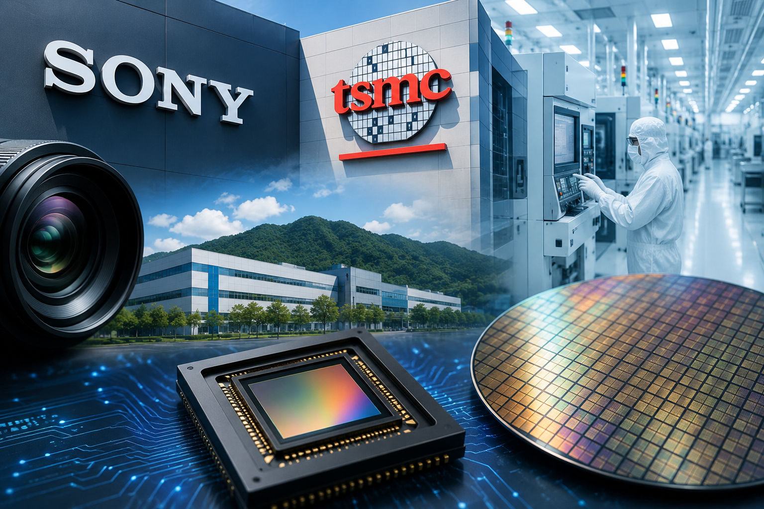
Joint venture to combine Sony’s image-sensor expertise with TSMC’s advanced manufacturing technology; commercial production could begin in Japan by 2029
Sony Group and Taiwan Semiconductor Manufacturing Company (TSMC) are planning to invest around 1 trillion yen, or $6.32 billion, in a joint project to manufacture next-generation microchips used in image sensors, according to a Nikkei report.
The proposed investment marks a significant expansion of the technology partnership between the two semiconductor giants and could strengthen Japan's position in advanced semiconductor manufacturing.
The joint venture is expected to be owned approximately 60% by Sony and 40% by TSMC, with commercial production potentially beginning as early as 2029 in Japan's Kumamoto prefecture. Reuters reported that Sony declined to comment on the Nikkei report, while TSMC had not immediately responded to a request for comment.
Sony and TSMC Bring Complementary Strengths
The proposed partnership brings together two companies with highly complementary capabilities.
Sony is the world's largest manufacturer of image sensors, which are widely used in smartphones, automobiles and other electronic devices.
TSMC is the world's largest contract semiconductor manufacturer and has extensive expertise in advanced chip fabrication and process technology.
The combination could allow Sony to strengthen its next-generation sensor technology while using TSMC's manufacturing capabilities to produce sophisticated chips at scale.
The two companies had already announced plans in May to establish a joint venture in Japan focused on developing and manufacturing next-generation image sensors.
$6.3 Billion Investment Highlights Strategic Importance
The size of the proposed investment demonstrates the increasing strategic importance of image-sensor technology.
Image sensors are no longer limited to conventional smartphone photography. They are becoming critical components in vehicles, industrial equipment, robotics, security systems and AI-powered machines.
As artificial intelligence moves beyond data centres and into the physical world, machines need increasingly sophisticated sensors to understand their surroundings.
This creates a long-term opportunity for companies that can combine sensor design, semiconductor manufacturing and AI-related technologies.
Commercial Production Could Start in 2029
The joint venture is expected to target commercial production as early as 2029 at a facility in Kumamoto, southern Japan.
The timeline means the project is primarily a long-term strategic investment rather than an immediate earnings catalyst for either company.
The partners will need to move through technology development, facility construction, equipment installation, testing and production ramp-up before commercial volumes can be achieved.
Execution will therefore be an important factor in determining the ultimate economic value of the investment.
Japan Emerges as a Key Semiconductor Manufacturing Hub
The planned investment also strengthens Japan's position in the global semiconductor supply chain.
Japan has been actively encouraging investment in advanced semiconductor manufacturing as countries seek to reduce dependence on concentrated chip-production hubs.
TSMC already has a significant manufacturing presence in Kumamoto, making the region increasingly important to Japan's semiconductor strategy.
A Sony-TSMC facility could benefit from the existing ecosystem of semiconductor suppliers, engineering capabilities and supporting infrastructure in the region.
Why Image Sensors Are Becoming More Important
Image sensors convert light into digital information that can be processed by electronic systems.
In smartphones, they are responsible for capturing images and video. But their applications are expanding rapidly.
Advanced image sensors are increasingly important for:
-
Automotive cameras
-
Driver-assistance systems
-
Autonomous vehicles
-
Industrial automation
-
Robotics
-
Security systems
-
Smart devices
-
Machine vision
-
AI-enabled physical systems
As these applications become more sophisticated, demand is shifting towards sensors capable of higher resolution, faster processing and improved performance in challenging environments.
Automotive Could Become a Major Growth Market
The automotive sector represents one of the biggest opportunities for advanced image sensors.
Modern vehicles increasingly use cameras for functions such as lane detection, object recognition, parking assistance and driver monitoring.
As vehicles move towards higher levels of automation, the number and sophistication of sensors required could increase further.
Sony and TSMC have specifically identified automotive applications as an area they intend to explore through their partnership.
This could provide Sony with a significant opportunity to expand beyond its traditional smartphone-related sensor business.
Robotics and Physical AI Open a New Market
The partnership will also explore applications involving physical artificial intelligence, particularly robotics.
Physical AI refers to systems that can perceive and interact with the real-world environment.
Robots require sensors to identify objects, understand their surroundings and make decisions based on changes in their physical environment.
As industrial and service robotics become more advanced, the need for high-performance image sensors could increase significantly.
The combination of Sony's sensing capabilities and TSMC's semiconductor manufacturing expertise could therefore position the partnership for a potentially important role in the emerging physical-AI ecosystem.
Sony Could Strengthen Its Image Sensor Leadership
Sony's semiconductor business is strategically important to the company, with image sensors representing a major area of expertise.
The company has invested heavily in sensor technology as smartphone manufacturers continue to demand better camera performance.
The next phase of growth, however, could increasingly come from markets beyond smartphones.
Automotive, robotics and industrial applications could diversify Sony's image-sensor revenue base and reduce its dependence on consumer-electronics cycles.
The partnership with TSMC could help Sony increase its manufacturing capabilities while continuing to focus on sensor technology and product development.
TSMC Expands Its Manufacturing Footprint in Japan
For TSMC, the project would further deepen its presence in Japan.
TSMC is best known for manufacturing advanced processors for smartphones, computing and artificial intelligence applications.
Its collaboration with Sony provides exposure to another important semiconductor category.
The partnership could also strengthen TSMC's relationship with Japan's technology and manufacturing ecosystem.
Japan’s Semiconductor Strategy Gets Another Boost
The project comes at a time when Japan is attempting to rebuild its semiconductor capabilities.
The global chip shortage and supply-chain disruptions of recent years highlighted the risks associated with excessive dependence on a limited number of manufacturing locations.
Governments around the world have responded by encouraging semiconductor investment within their borders.
Japan has similarly sought to attract advanced chip manufacturing and strengthen domestic supply chains.
The Sony-TSMC project fits directly into this broader strategy.
Semiconductor Supply-Chain Diversification Gains Momentum
The global semiconductor industry is increasingly moving towards geographic diversification.
Companies and governments are seeking manufacturing capacity across multiple regions to reduce exposure to geopolitical tensions, trade restrictions and supply disruptions.
Japan offers several advantages, including a sophisticated electronics industry, a strong manufacturing base and a large network of semiconductor-related suppliers.
The expansion of semiconductor production in Kumamoto could therefore have benefits beyond Sony and TSMC.
Smartphone Demand Remains an Important Driver
Despite the growing importance of automotive and robotics, smartphones remain a major market for image sensors.
Premium smartphones are increasingly equipped with multiple cameras and sophisticated imaging systems.
Consumers continue to demand improvements in:
-
Low-light photography
-
Dynamic range
-
Video quality
-
Autofocus
-
Computational photography
-
High-resolution imaging
This creates a continuing need for more advanced image sensors.
However, the longer-term opportunity could increasingly shift towards applications where cameras are used not merely to capture images but to help machines understand the physical world.
The Rise of Machine Vision
Machine vision represents another potentially important market.
Factories increasingly use cameras and sensors for automated inspection, quality control and robotics.
As manufacturers adopt more automation, sophisticated image sensors can help machines identify defects, monitor production lines and interact with objects.
This could create demand for sensors designed specifically for industrial environments.
Sony's sensor technology could therefore benefit from the broader automation trend.
The Project Is More Than a Manufacturing Partnership
The Sony-TSMC relationship could ultimately extend beyond manufacturing.
The companies have indicated that they will explore opportunities involving physical AI, automotive technology and robotics.
This suggests that the partnership is designed around the broader convergence of semiconductors, sensors and artificial intelligence.
That convergence could become increasingly important as AI moves from software applications into physical devices.
Major Long-Term Opportunities
The partnership provides exposure to several structural technology trends.
Artificial Intelligence
AI is expanding from cloud computing into physical devices, increasing demand for sensors and edge computing.
Autonomous Vehicles
More sophisticated vehicle automation requires increasingly capable camera and sensor systems.
Robotics
Industrial and service robots need advanced perception capabilities.
Smart Devices
Connected devices increasingly rely on cameras and sensors to understand their environment.
Industrial Automation
Factories are using machine vision and AI-powered systems for inspection, monitoring and production.
Key Challenges Ahead
Despite the long-term opportunity, the project faces several challenges.
Execution Risk
Building and ramping a sophisticated semiconductor manufacturing facility can involve significant technical and operational complexity.
Capital Requirements
The proposed investment of around $6.32 billion represents a substantial commitment, making efficient capital deployment important.
Technology Development
Next-generation image sensors must deliver meaningful improvements in performance while remaining commercially viable.
Market Adoption
The long-term success of the project will depend on the pace at which automotive, robotics and other industries adopt advanced sensor technologies.
Competitive Pressure
The image-sensor and semiconductor markets remain highly competitive, with technological development occurring rapidly.
What the Investment Means for Japan
The project could have wider implications for Japan's technology ecosystem.
A major semiconductor investment can create demand for suppliers, equipment manufacturers, engineers and other specialised services.
The development of a larger semiconductor cluster in Kumamoto could also encourage additional investment from companies operating across the chip supply chain.
Over time, this could strengthen Japan's position in advanced semiconductor manufacturing.
Market Outlook
The Sony-TSMC investment represents a long-term strategic positive for the global semiconductor and image-sensor industries, particularly as AI, robotics and autonomous vehicles expand.
The proposed $6.32 billion investment combines Sony's leadership in image sensors with TSMC's advanced manufacturing capabilities, creating the potential for next-generation sensor technology to be deployed across a much wider range of applications.
For Sony, the partnership could strengthen its position in image sensors while opening additional growth opportunities in automotive, robotics and industrial applications.
For TSMC, the project provides another opportunity to expand its manufacturing footprint in Japan while participating in the growing convergence between semiconductor technology and physical AI.
The planned 2029 commercial-production timeline means the immediate financial impact is likely to be limited. The more important developments will be the progress of the joint venture, construction and technology development, followed by production ramp-up and customer adoption.
The broader investment thesis, however, remains compelling. As AI increasingly moves into vehicles, robots, factories and other physical environments, the ability of machines to accurately see and interpret the world around them will become increasingly important.
That makes advanced image sensors a potentially critical component of the next phase of the AI and semiconductor cycle, while the Sony-TSMC partnership could become an important part of Japan's efforts to strengthen its position in the global chip supply chain.